



半导体设备 Semiconductor Equipment
HURAKAN深耕高端精密半导体设备工业设计领域,熟稔半导体生产车间无尘、恒温、高精密度的严苛工况标准,精通精密设备结构工艺、无尘车间适配规范与量产落地逻辑。针对半导体设备项目,团队完成从行业场景调研、产品定位规划、外观创意设计、精密结构迭代、人机体验优化到样机验证、量产对接的全流程闭环服务。深度结合晶圆加工、检测封装等半导体核心工艺场景,针对性解决传统半导体设备外观杂乱、结构集成度低、运维繁琐、人机适配性弱等行业痛点,全程协同客户研发、工艺、生产团队完成结构校核、无尘适配调试与量产工艺优化,以严谨的工科思维和丰富的高端精密设备落地经验,保障设计方案合规、稳定、可量产,全方位彰显团队扎实、靠谱的专业化落地交付能力。
Specializing in the industrial design of high-end precision semiconductor equipment, HURAKAN is familiar with the stringent operating standards of dust-free and constant-temperature semiconductor production workshops with high precision requirements, and proficient in precision equipment structural technology, dust-free workshop adaptation specifications and mass production landing logic. For the semiconductor equipment project, the team provides full-process closed-loop services including industry scenario research, product positioning planning, creative appearance design, precision structure iteration, human-machine experience optimization, prototype verification and mass production docking. Deeply adapting to core semiconductor process scenarios such as wafer processing, inspection and packaging, we solve industry pain points of traditional semiconductor equipment such as messy appearance, low structural integration, cumbersome maintenance and weak human-machine adaptability. We cooperate with clients’ R&D, process and production teams throughout the whole process to complete structural verification, dust-free adaptation debugging and mass production process optimization. With rigorous engineering thinking and rich experience in landing high-end precision equipment, we ensure all design schemes are compliant, stable and mass-producible, fully demonstrating the team’s solid and reliable professional delivery capability.
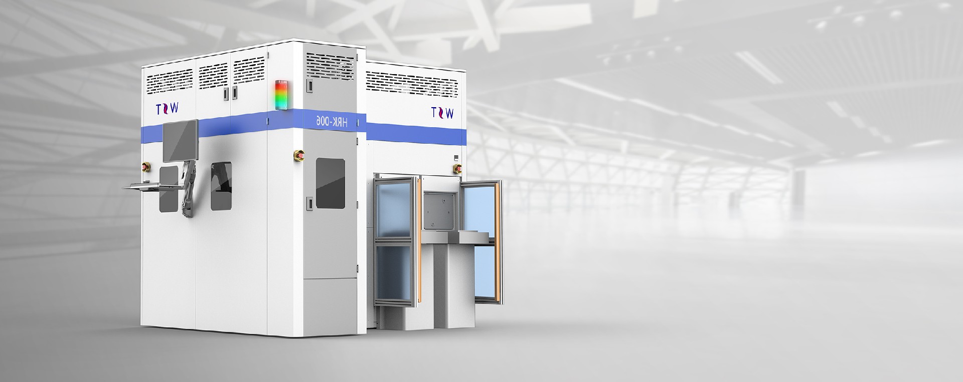
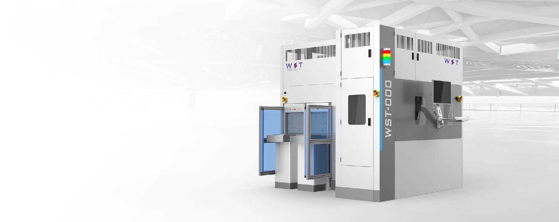
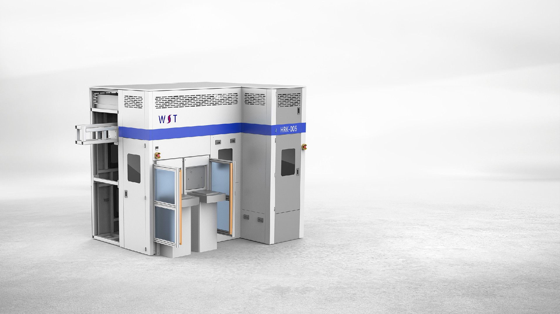
在造型设计上,团队打破传统半导体设备线条杂乱、柜体臃肿、工业质感粗糙的同质化弊端,贴合半导体无尘车间极简、规整、智能、精密的高端空间调性,打造一体化极简精密柜体造型。整机采用对称均衡的柜体比例,搭配平整利落的曲面过渡与隐藏式走线设计,摒弃多余外露结构,视觉干净规整、层次高级,充分凸显精密设备的专业质感;配色采用工业高端低饱和哑光色系,适配无尘车间洁净标准,具备防尘、抗静电、易擦拭消杀的核心属性,兼顾美观性与工业实用性。以极简统一的外观设计语言摆脱行业低端同质化内卷,塑造高精度、智能化、现代化的半导体设备视觉标签,适配各类高端半导体生产与研发场景。
In terms of styling design, the team breaks the homogenization drawbacks of traditional semiconductor equipment such as messy lines, bloated cabinets and rough industrial texture. In line with the high-end spatial tone of minimalist, regular, intelligent and precise dust-free semiconductor workshops, we create an integrated minimalist and precise cabinet shape. The whole machine adopts symmetrical and balanced cabinet proportions with neat curved transitions and hidden wiring design, eliminating redundant exposed structures to present a clean, regular and advanced visual level and highlight the professional texture of precision equipment. The high-end industrial low-saturation matte color scheme complies with the cleanliness standards of dust-free workshops, with core attributes of dust resistance, anti-static performance and easy cleaning and disinfection, balancing aesthetics and industrial practicality. The minimalist and unified appearance design language gets rid of low-end industry homogenization involution, shapes a visual label of high-precision, intelligent and modern semiconductor equipment, and adapts to various high-end semiconductor production and R&D scenarios.
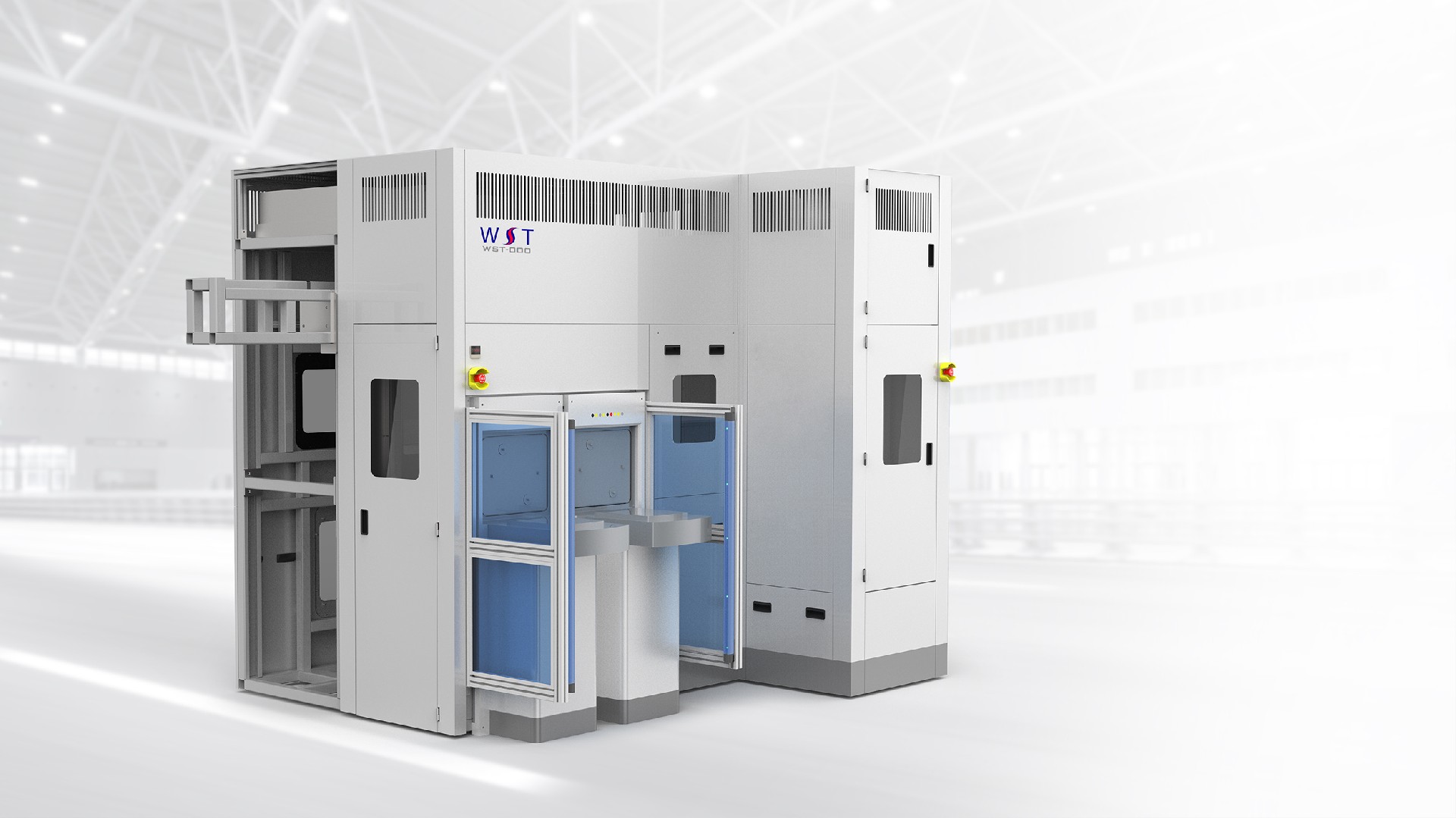
结构设计围绕高精密度运行、无尘环境适配、长效稳定作业、轻量化便捷运维四大核心需求开展创新优化,实现精密性能与量产实用性的高度平衡。团队重构设备模块化分层布局,科学划分工艺处理区、电控散热区、精密检测区,实现功能分区独立隔离,有效规避粉尘堆积、热量聚集、电磁干扰等问题,从结构层面保障半导体加工与检测的高精度、高稳定性;优化整机密封、防尘、防静电结构,完全适配无尘车间严苛生产标准,杜绝外界因素影响产品良率。同时创新采用分体式模块化拆装结构,核心精密组件、易损部件可独立拆卸检修与更换,大幅降低设备运维难度与停机损耗,整体结构适配大型精密设备量产工艺,有效平衡产品品质与生产成本。
The structural design carries out innovative optimization focusing on the four core requirements of high-precision operation, dust-free environment adaptation, long-term stable operation and lightweight convenient maintenance, realizing a high balance between precision performance and mass production practicality. The team reconstructs the modular layered layout of the equipment, scientifically divides the process processing area, electric control heat dissipation area and precision detection area, and realizes independent isolation of functional zones, effectively avoiding dust accumulation, heat aggregation and electromagnetic interference, and ensuring the high precision and stability of semiconductor processing and detection from the structural level. The optimized overall sealing, dust-proof and anti-static structure fully adapts to the strict production standards of dust-free workshops and eliminates external factors affecting product yield. Meanwhile, the innovative split modular disassembly structure enables independent disassembly, inspection and replacement of core precision components and vulnerable parts, greatly reducing equipment maintenance difficulty and shutdown loss. The overall structure adapts to the mass production technology of large-scale precision equipment, effectively balancing product quality and production cost.
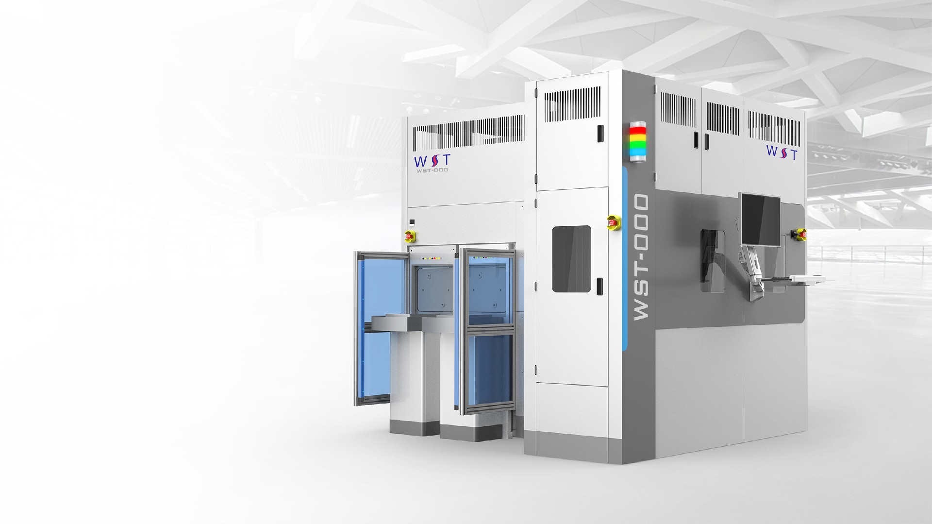
人机交互设计深度贴合半导体车间操作人员、工程师的长期作业与设备调试场景,全方位优化操作效率、作业安全与使用体验。设备操控终端采用人体工学前倾倾角设计,适配工作人员站姿常态化操作视角,有效缓解长时间调试、参数校准带来的视觉与肢体疲劳;重构可视化操作界面逻辑,简化复杂工艺参数设置、设备状态监测、故障排查、数据记录等功能层级,界面直观清晰、操作逻辑简洁,大幅降低精密设备的操作门槛与人为失误率。同时优化机身检修口、操作面板的布局位置,贴合人体操作动线,兼顾日常简易操控与深度运维调试需求,适配半导体车间高强度、高精度的常态化作业模式。
The human-machine interaction design is deeply adapted to the long-term operation and equipment debugging scenarios of operators and engineers in semiconductor workshops, comprehensively optimizing operation efficiency, operational safety and user experience. The equipment control terminal adopts an ergonomic forward-tilt angle design, fitting the normal standing operation perspective of staff and effectively relieving visual and physical fatigue caused by long-term debugging and parameter calibration. We reconstruct the logic of the visual operation interface, simplify the functional levels of complex process parameter setting, equipment status monitoring, troubleshooting and data recording with an intuitive interface and concise operation logic, greatly reducing the operation threshold and human error rate of precision equipment. At the same time, we optimize the layout position of the fuselage maintenance port and operation panel to fit the human operation route, meet the needs of daily simple control and in-depth maintenance and debugging, and adapt to the high-intensity and high-precision normalized operation mode of semiconductor workshops.
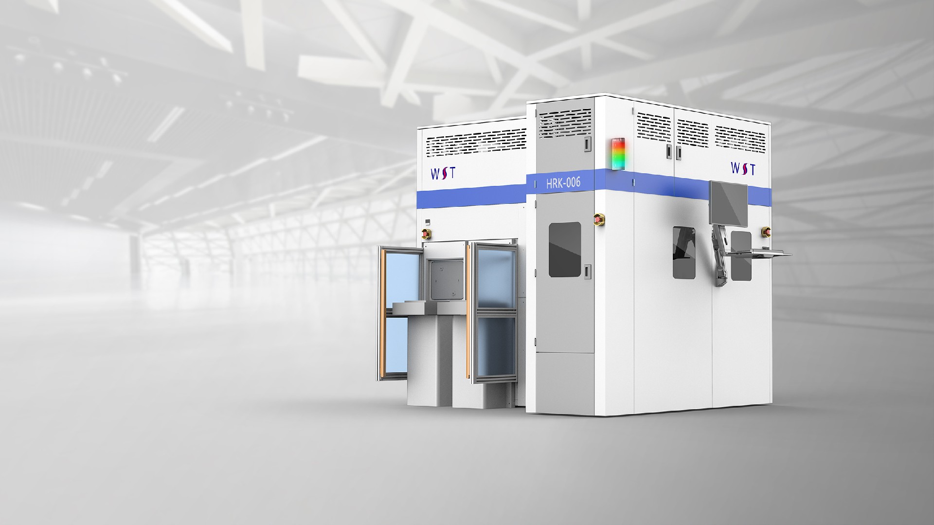
依托HURAKAN对高端精密工业设备的设计积淀与全流程落地赋能能力,这款半导体设备实现了外观美学、结构精密性、工况适配性与人机体验的全方位迭代升级,彻底打破传统半导体设备造型老旧、体验粗糙、运维低效的行业短板,构建强有力的产品差异化竞争优势。产品量产落地投入市场后,凭借高标准无尘适配性能、稳定精密的作业表现、高端精致的外观质感与低运维成本,助力客户顺利切入中高端半导体设备赛道,快速抢占上下游优质供应链资源。产品有效摆脱行业低价竞争格局,实现显著市场溢价,大幅提升终端产品销量与品牌市场渗透率,持续强化客户在精密半导体设备领域的核心竞争力,完成从设计创新、产品差异化到商业增值与品牌升级的完整价值闭环。
Relying on HURAKAN's design accumulation and full-process landing empowerment capabilities for high-end precision industrial equipment, this semiconductor equipment has achieved all-round iterative upgrades in appearance aesthetics, structural precision, working condition adaptability and human-machine experience, completely breaking the industry shortcomings of traditional semiconductor equipment such as outdated shape, rough experience and inefficient maintenance, and building strong product differentiated competitive advantages. After mass production and market launch, with high-standard dust-free adaptation performance, stable and precise operation performance, high-end exquisite appearance texture and low operation and maintenance cost, the product helps clients successfully enter the mid-to-high-end semiconductor equipment track and quickly seize high-quality upstream and downstream supply chain resources. It effectively gets rid of the industry's low-price competition pattern, achieves significant market premium, greatly improves terminal product sales and brand market penetration, continuously strengthens clients' core competitiveness in the field of precision semiconductor equipment, and realizes a complete value closed loop from design innovation and product differentiation to commercial appreciation and brand upgrading.



Microblog